


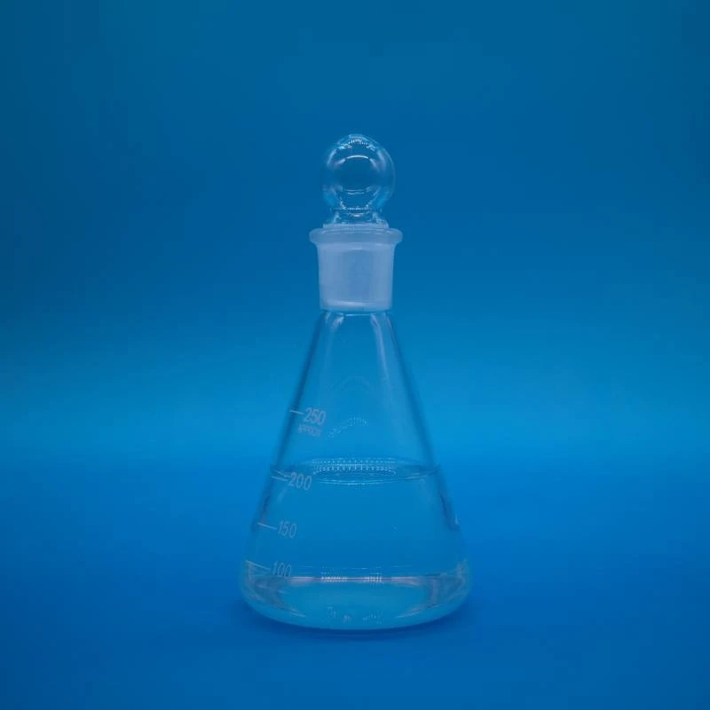
Shandong Peak-tech New Material Co., Ltd. is one of the most reliable manufacturers and suppliers of colloidal silica for semiconductor in China. With a professional production team, we are able to meet the needs of the majority of our customers. Welcome to buy durable colloidal silica for semiconductor for sale here from our factory.
Colloidal Silica for Semiconductor Grade Comparison
| Model | Particle Size | SiO₂ Content | Metal Ions | pH | Shelf Life |
|---|---|---|---|---|---|
| HP25D10 | 10–20 nm | 25±1% | <20 ppm | 7–9 | ≥12 months |
| HP3010 | 10–20 nm | 30±1% | <50 ppm | 7–9 | ≥12 months |
| HP2510A | 10–20 nm | 21–25% | <50 ppm | 2–4 | ≥12 months |
| HP4010A | 10–20 nm | 38–42% | <50 ppm | 2–4 | ≥12 months |
Aluminum present as Al₂O₃ is excluded from the listed metal-ion total. HP25D10 and HP3010 are NH₄⁺-stabilized. Semiconductor qualification requires element-specific limits, clean handling and process-specific validation beyond the published total.
Build the Specification Around Contamination Risk
Lowest Published Metal Total
HP25D10 provides the tightest aggregate metal-ion limit among the listed semiconductor candidates.
Set Element-Specific Limits
Specify sodium, iron, aluminum and other process-sensitive elements individually, with methods and detection limits.
Control Distribution and Agglomerates
All four grades share a 10–20 nm range. Confirm PSD, oversized-particle limits, agglomerates and the measurement method.
Match Stabilizer and pH
Select an acidic or near-neutral grade according to process chemistry, permitted ions and surrounding materials.
Information Needed for Semiconductor Qualification
Semiconductor approval requires contamination, particle, packaging, lot-control and change-management criteria beyond the product-family table.
- Elemental limits: provide maximum values for each controlled metal and the reporting basis.
- Analytical methods: specify ICP-MS, ICP-OES or other required methods, detection limits and sample preparation.
- Particle specification: define nominal size, distribution, agglomerate limit and metrology method.
- Process chemistry: confirm application, SiO₂ content, pH, stabilizer, conductivity and permitted ionic species.
- Lot and change control: state COA fields, sampling rules, retention samples, traceability and change-notification requirements.
- Packaging: define container material, cleanliness, filtration, filling environment, trial quantity and destination.
Request Colloidal Silica for Semiconductor Qualification
Send the application, element limits, particle specification, analytical methods, packaging and lot-control requirements.
Request Qualification SupportProtect Product Stability During Storage
Packaging Options
Available polyethylene packaging sizes are 25 kg, 250 kg and 1000 kg.
Storage Temperature
Store at 0–40°C and protect from freezing. Temperatures below 0°C can cause irreversible gelation.
Direct Sunlight
Avoid prolonged exposure to direct sunlight during storage and transportation.
Container Closure
Keep containers closed to limit water evaporation and precipitation of solid silica particles.
Colloidal Silica for Semiconductor Questions
Which colloidal silica grades can be evaluated for semiconductor use?
The high-purity candidate grades are HP25D10, HP3010, HP2510A and HP4010A.
Which semiconductor candidate has the lowest published metal-ion total?
HP25D10 is listed below 20 ppm; the other published HP grades are listed below 50 ppm.
Is the published total metal-ion value sufficient for semiconductor qualification?
Not always. Buyers should define element-specific limits, analytical methods, detection limits and reporting basis.
What clean-packaging requirements should be defined?
Define container material, particle cleanliness, filtration, filling conditions, sealing, sampling and transport requirements.
What lot-control documents should semiconductor buyers request?
Define required COA fields, test methods, sampling rules, retention samples and change-notification expectations before qualification.
Hot Tags: colloidal silica for semiconductor, China colloidal silica for semiconductor manufacturers, suppliers, factory
Applications of Colloidal Silica for Semiconductor
HP grades can be evaluated for semiconductor-related materials and precision processes after element limits, particles, process chemistry, packaging and lot controls are agreed.
Semiconductor CMP
Evaluated as an abrasive dispersion where particle control, metal contamination and slurry chemistry are tightly specified.
Wafer and Substrate Polishing
Suitable candidates can be tested for compatible ceramic, glass and other precision electronic substrates.
Semiconductor Packaging Materials
High-purity grades may be assessed in compatible packaging-material formulations where trace metals and particles are controlled.
Precision Electronic Surfaces
Controlled nanosilica can be qualified for compatible precision-finishing and functional-material processes.
High-Purity Inorganic Coatings
Selected candidates may be evaluated in compatible inorganic coatings requiring controlled metals and particle specifications.
Custom Semiconductor Materials
Supports development requiring defined element limits, particle metrology, traceability, change control and clean packaging.


